Dragon Development Board
It is a low cost development board that lets you embed Linux into your projects. It runs OpenWrt with a Linux kernel, has 2 USB host ports and has full Ethernet and 802.11 b/g/n WiFi capabilities.
Applications:
- Internet of Things
- Voice over IP
- Mesh WiFi
- Industrial Control
- Internet Radio
- 3G/4G router
OpenWrt is a reliable Linux distribution for embedded systems with an emphasis on networking. It is open source, actively developed and well maintained. OpenWrt uses the OPKG package system, has lots of powerful utilities and the software is maintained in package form. Users can easily install, add and remove packages to make a very customized system.
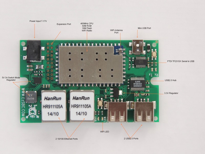
AR9331 OpernWrt Development Board
Specifications:
CPU: ATHEROS AR9331 chipset, which integrates MIPS 24Kc processor, CPU 400MHz, Hardware Ethernet Switch (MAC, PHY) and integrates with on chip MAC, RF, PA and LNA for WiFi.
RAM : 64MB;
Flash : 16MB
Interfaces: 2 x RJ45, 2 x USB Host, 1 x UART, 14 GPIOs
OS: Linux based OpenWrt
Power: 7 to 17 VDC power input with onboard switch mode regulator
WiFi: Support 150M 2.4Ghz WiFi, 802.11 b/g/n
Frequency range: 2.4~2.4835GHz
Modulation: BPSK, QPSK, CCK and OFDM (BPSK/QPSK/16-QAM/ 64-QAM)
Sensitivity @PER : 135M : -65dBm@10%PER; 65M : -65dBm@10%PER; 54M : -68dBm@10%PER; 11M : -84dBm@8% PER; 6M : -88dBm@10% PER; 1M : -90dBm@8% PER
Typical Distance: Indoor: 60m (max); Outdoor 150m (max) (with 2 dBi antenna)
RF Power: 11n: 13dBm; 11g: 13-15dBm, 11b: 16-18dBm,
Antenna Connector: I-PEX connector.
Why?
The board was developed as an alternative to hacking a commercial router such as the TP-Link TL-WR703N Mini Portable Wireless Router to use as a development platform. There are many routers available based on the Atheros AR9331 Chipset and running customized versions of OpenWrt or DD-Wrt software. The TL-WR703N is popular because of its low price and small size.
Hacking a router to install OpenWrt is a well tried path to getting a functional board with open source software to allow development of low volume or one-off projects. It has its problems. In most cases the schematics are not available unless someone took the trouble to reverse engineer the schematics from the printed circuit board. The TL-WR703N has been reverse engineered and the schematics are available here . I looked at the schematics and they appear reasonable and are most likely correct or nearly so. So again, why bother making a board based on the same chipset? Part of the answer lies in our own requirements. We wanted a board with more than one Ethernet port and a USB port to allow us to write data on a real hard drive. The Raspberry Pi and the Beaglebone fail the two Ethernet port requirement although they have lots of USB ports available. In some cases we want to turn off the radio and use only the wired ports for security reasons. Also, routing Ethernet packets without hardware assistance is a CPU killer in terms of work load. That still leaves the option of using a commercial router and hacking it.
There are many routers out there and may are well supported by OpenWrt, our preferred operating system. Many have four or five Ethernet ports and some have USB ports as well. Some testing has shown that we need 64M of RAM for our target application and that ruled out some routers. The lower cost routers all seemed to be based on the AR9331 system on a chip and some testing on hacked boards lead to a remarkably annoying discovery. You can have two identical routers with identical software and one will have a reliable USB port, one not. Even worse, some have very low failure rates so they appear OK but will hang when left unattended.
Searching on the Internet for a fix showed that OpenWrt has a patch for the problem. After making sure the patch was applied we tested a couple of boards and they worked well. In fact, they worked so well that we considered the problem solved and started developing the application. After some time a board that worked correctly acted up and would not be reliable with a hard disk attached to the AR9331 USB port. We had previously tested this exact board with a hard drive and copied very large amounts of data from one place on the drive to another. We also read the content of the entire drive, a few hundred gig without any problem whatsoever. I tried another board with a physical hard drive and it worked fine but it absolutely refused to read an old USB Flash drive. Searching on the Internet for a solution I saw a post somewhere that installing a passive USB hub between the chipset USB port and the drive (or keyboard, USB to UART adapter or some other devices) fixes the problem for some people. We tried it and it worked! A flaky USB system became reliable. Two questions remained; Is it really fixed? and What is the cause? There is a large topic on the OpenWrt forum that started in 2012 and is still going about this USB issue. https://forum.openwrt.org/viewtopic.php?id=39956 There were many theories and suggestions including reading undocumented registers and writing the contents back periodically. More searching and emails eventually crystallized into the following facts:
- All AR9331 devices have a USB stability issue
- It is not power supply related
- Disabling the WiFi makes the problem go away
- The problem can be solved by adding a USB 2.0 Hub between the AR9331 and the offending devices
- USB 1.1 devices never work reliably.
The problem seems to be due to a hardware bug in the AR9331 and terminology problems. The AR9331 has a USB2.0 controller and it works reliably with USB 2.0 devices (only) but is unreliable with USB 1.1 or Full Speed USB devices. The problem can be resolved in hardware by installing a hub that connects to the AR9331 as a high speed USB 2.0 device and translates USB 1.1 transactions to USB 2.0 transactions.
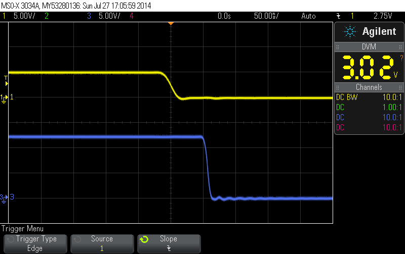
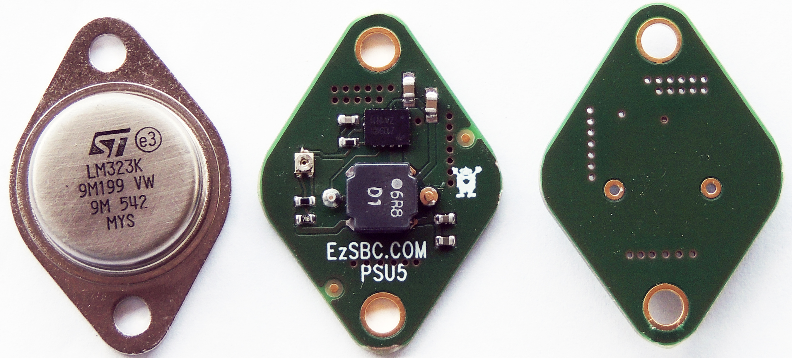
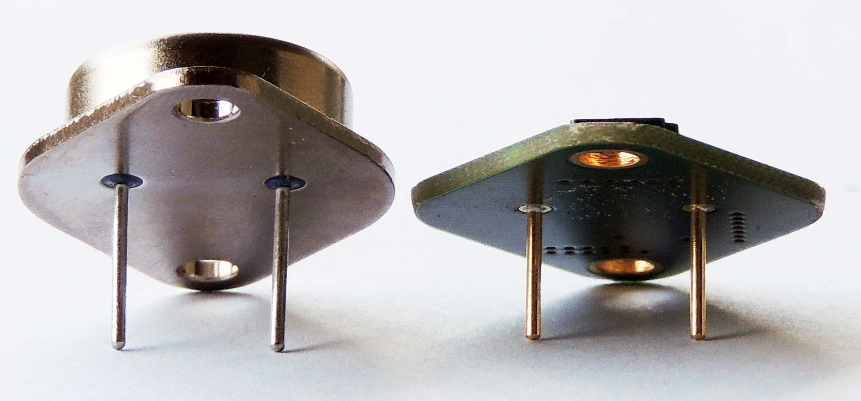
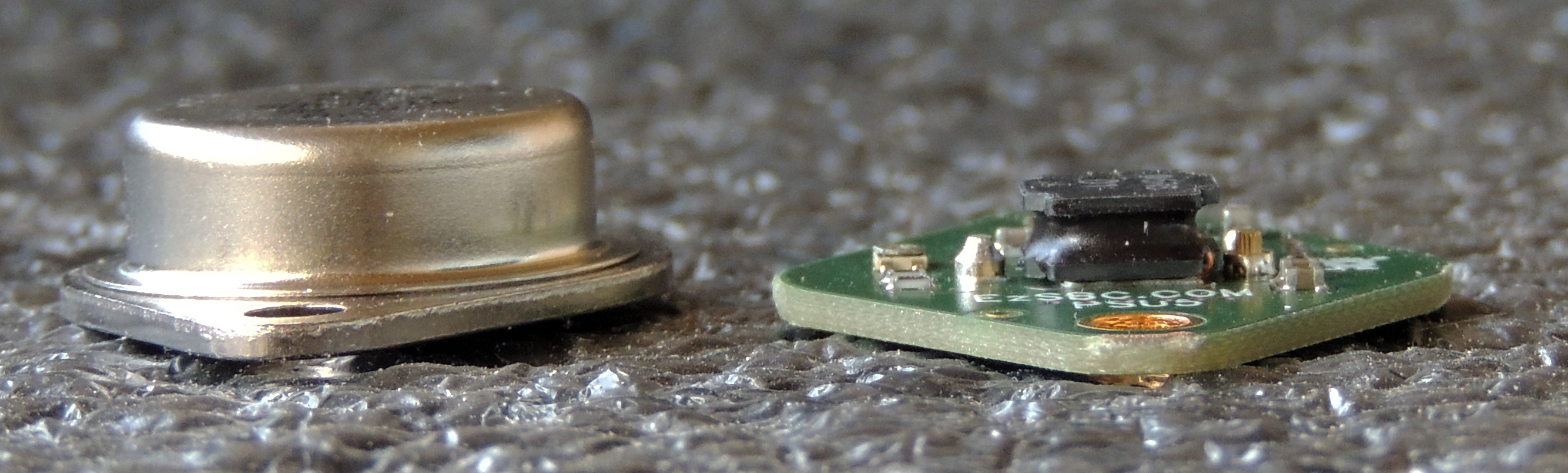
I added a USB 2.0 Hub to the board and for good measure I added a second USB host port as well. We now have reliable USB ports for anything recognized by the software. Since one of our aims is to use physical hard drives attached to the USB ports I added a 5V 3A switch mode regulator to the board and wired the 5V directly to the two USB host ports. The ports don’t respect the 100mA/500mA current limits of standard USB port and will happily supply 2A or more on a port as long as the total current drain is less than 3A.
The board has been undergoing testing now for a couple of weeks and it appears that all the bugs are now in the software. All the parts are in house but the solder paste stencil is still in process. The board will be available for purchase by the end of June 2015 and a single unit will be below $50.