Some people noticed that the first Power Supply Module to appear on the site was named PSU2. This oddity was due to design named PSU1 turned out to be remarkably difficult to assemble with a decent yield. The PSU2 was designed to fill the immediate need for 5V and 3.3V switching regulators that are drop in replacements for linear three pin regulators such as the 7805 but without the headache of the heatsink. This is particularly true when the supply voltage is 12V. Even at 500mA load current the heatsink is embarrassingly large. The design of the PSU2 was done in a short time and it is a very successful design that has very low ripple and noise. The switching frequency is high to keep the filter components small. The two limitations of the PSU2 is that the input voltage range is restricted to 17V maximum and that is less than the original 7805 family and the highest output voltage available is 5V, again lower than the original 7800 family.
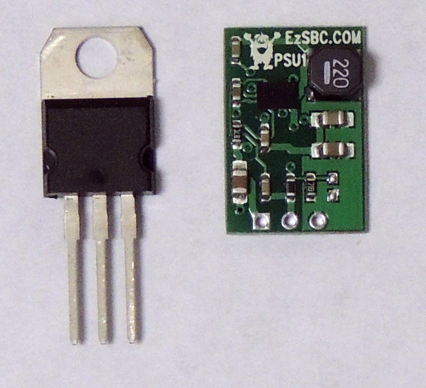
The PSU1 design overcomes these limitations while keeping the same form factor as the PSU2. The only difference in the mechanical size is the PSU1 has a larger inductor.
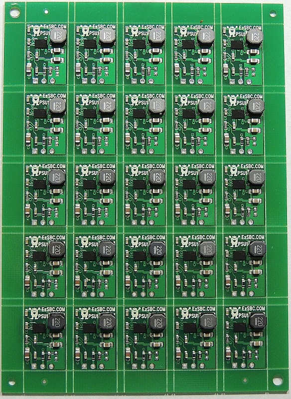
The photograph above shows a panel of the PSU1 design after reflow and test. This was the third panel assembled and the first one with 100% yield. For those unfamiliar with assembly details this is a good example of the challenges of manufacturing small PCB’s on automatic equipment. To be able to place the components the Pick and Place machine needs some clearance to the edge of the board and must be able to hold the board. The strips on the outer edge are commonly referred to as ‘thieves’ (I don’t know why) and allow the machine to hold the pane and populate components up to the edge of the individual PCB’s. On these strips there are a few holes and copper dots. The dots are to allow the P&P machine to determine the exact position of the panel and to correct for variations in the routing of the panel. The dots are called ‘fiducial marks’ and are sometimes placed near fine pitch devices to allow for accurate placement of those IC’s. The vertical lines between the individual PCB’s are ‘v-scores’ to allow the boards to be separated after assembly and in this case after testing as well. There are limitations to the smallest size of board that can be scored and this panel can not be scored exactly next to the PCB’s due to these limitations. The small sections of board are inserted into the panel to allow the board edges to be scored even though the blades can not be set to the width of the individual PCB’s. By adding these small sections the board edges can be scored by passing the panel through the scoring machine twice.
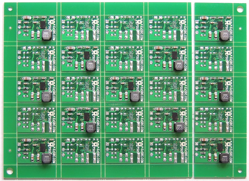
The holes on the corners of the panel to allow precise alignment in my solder paste printer. The printer has pins that exactly fit the holes and the repeatability from panel to panel is as good as the registration of the holes to the copper. To ensure proper soldering on this design was remarkably hard. The IC is a ball grid device with a fine pitch and it has to be mounted in close proximity to the inductor. The noise increases and efficiency decreases as the inductor is moved further away from the away from the IC. The mass of the inductor prevents that part of the board from heating as fast as the rest of the board and may lead to poor solder joints underneath the IC where it is impossible to inspect without x-rays. Solder paste consist of metal, flux and other magic sauce that gives it the properties required to print correctly, not slump after printing and solder properly. To judge the solder volume and alignment I made a test panel where the diagonals were populated with components and then it went through the reflow oven.
The photo above is of the partially populated panel after it went through the reflow oven. Note how small the dots are for the BGA part.
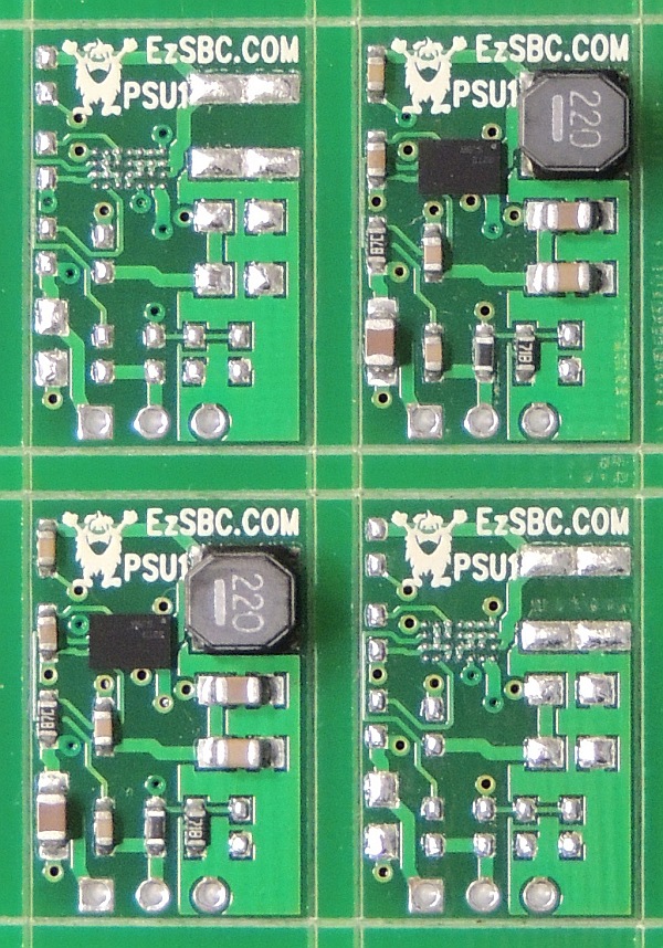
This is a photo showing a close-up of four boards with two populated and two unpopulated boards. With a microscope and some patience the solder volume on each pad can be calculated and the uniformity of the deposition can be evaluated. To limit the amount of paste placed on the inductor pads the stencil has two openings for each pad. I thought the paste would flow together but it clearly does not. In this case it does not matter because there is enough solder on the pads and once the inductor is placed in the paste it does solder uniformly. It does highlight the need to be sure that a QFN package is pressed down firmly enough into the solder to make sure the solder covers the entire pad underneath the IC since the solder does not seem to flow horizontally but prefers to make ‘bumps’. From this photograph it is also really easy to see how small and tightly spaced the balls are on this package.
This design has a 40V input limit and eventually there will be 9V and 12V variants available. For now the 5V and 3.3V are available in production quantities.
To emphasize how small the board is it is shown next to a LM7805.